


Printed circuit parameters
To make it easier for you to select the printed circuit board parameters. We would like to provide some technical information of a printed circuit board:
| Tiêu chuẩn kỹ thuật | Thông số | Hình ảnh |
|---|---|---|
| Số lớp (Floors) | 1-6 lớp | |
| Chất liệu bảng mạch (Sheet type) | FR4 | |
| Kích thước tối đa của bản mạch (Thinkness range) | 550 x 420 mm | |
| Độ rộng đường mạch tối thiểu (Minium line width) | 3 mil (=0,075mm) |  |
| Khoảng cách tối thiểu giữa hai đối tượng (Min trace spacing) | 4mil (0,1mm) Có thể nhỏ hơn nhưng sẽ phụ thêm phí |  |
| Kích thước lỗ khoan (Finished hole diameter) | 0,2-6,2mm |  |
| Phần hàn tối thiểu lỗ via (Vias unlateral weld ring) | >=6mil (0.153mm) | 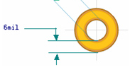 |
| Độ dày của chữ để in | >=0,15mm. Lưu ý để tên đẹp bạn hãy sử dụng thông số sau: Nét khung linh kiện là 0,3mm. Nét chữ linh kiện cao 2mm,nét chữ 0,18mm. Tên mạch cao 2,5mm,nét chữ 0.15mm | 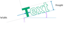 |
| Độ dày của lớp đồng | 35um/70um/105um (tương đương 1oz/2oz/3oz) | 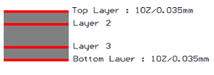 |
MỘT SỐ QUY ĐỊNH KHÁC:
- Đảm bảo kích thước lỗ khoan đúng và đặt trên đúng layer Drill.
- Vẽ đường biên trên layer Keep Out( Global, dimension …)
- Xác định chính xác mặt cắm LK và mặt hàn LK đối với board 1 mặt.
- Độ hở mở copper (phủ đồng) tối thiểu 16 mils=0.4mm
- Để tránh sai sót không đáng có trong quá trình gia công quý khách nên chuyển file thiết kế mạch in sang dạng
gerber
Related posts

What is the Printed Circuit?
Printed circuit board or printed circuit board (English: printed circuit board - PCB), sometimes referred to as printed circuit board, is a circuit board that...

What is SMT?
SMT stands for cluster of Surface Mount Technology (Technology of surface paste), in PCB technology, it is called welding technology for paste components, since 2008...

Read electronic diagrams
For an electrical and electronic technician, it is important to know how to read and understand electronic circuit diagrams to develop this broad field. If...
New post
What is the Printed Circuit?
3/07/2019
Read electronic diagrams
3/07/2019

FR4 – materials used in printed circuits
3/07/2019
What is SMT?
3/07/2019

Printed circuit parameters
3/07/2019


